Thin Films of Optical Materials
The field of optical materials is an actively developing field given that besides classical waveguides also advanced photonic band gap structures can be built. Miniaturisation and integration of the optical devices impose substantial opportunities and challenges – e.g. shaping the right material into the right form is not always an easy task. We address this challenge in our lab by developing methods of fabrication and processing of optical materials for integrated optics.
The high vacuum chemical vapour deposition technique (HVCVD) for deposition of thin films of oxide materials has been developed in our group during many years. Our HVCVD reactor is designed for 4” wafers, which can be heated up to 700°C. Three independent precursor delivery lines are available at the reactor. Precursor behaviour in high vacuum may significantly differ from the one observed in standard CVD conditions. Precursor testing and selection is an important part of our expertise and research interest. Various electro-optical materials for active laser properties and waveguides have been developed. Among the materials we are working with are LiNbO3, BaTiO3, TiO2, Al2O3, Nb2O3, HfO2.
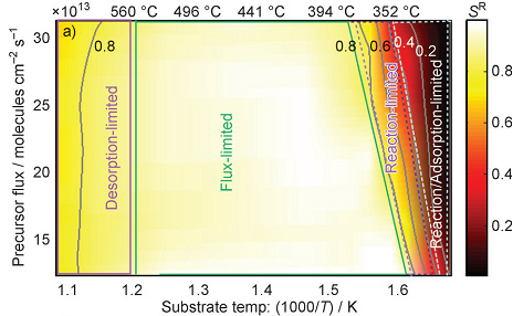
Deposition efficiency of Nb(ethox)4dmae precusor depending on flux and temperature.
(ChemPhysChem2011, 12, 3524–8)
Characterization of structural and functional properties of thin films is also an important task in the investigations and provides feedback for the fabrication process. Currently, we are working on the integration of crystalline materials such as LiNbO3 and BaTiO3 into different substrates to enable up scaling. Processing methods of thin films on the wafer scale, such as structuring, selective deposition with irradiation by laser or electron beam, lift-off techniques are critical aspects of integration and device fabrication and receive high attention from us.
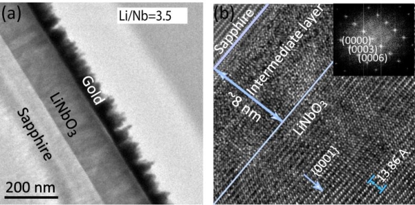
Transmission electron microscopy (TEM) image of LiNbO3 thin film – substrate interface.
(J. of Electrochem. Soc., 1582
Industrial Laser Processing
Our laboratory actively carries out research on laser processing of materials in the frame of two industrial mandates. We have wide experience in analysis and understanding of dynamics of laser prcessing as well as light-material interactions.
In one of the projects we developed together with an industrial partner a laser sintering process of ceramic materials on a substrate surface for marking applications. Parameters for sintering of ceramics on glass and metal as substrates are being investigated.
Our second industrial project looks to optimizing laser processing of hard materials. We focus in particular on laser cutting of diamond and hard-metal (tungsten carbide). EMPA is active in the analysis of the laser processing on the material and in the optimization of the range of cutting process parameters.
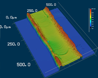
3D image of laser sintered/molten ceramic material.
Optical Defect Detection
We plan on developing industrially applicable optical methods for detection and investigation of features (defects or structures) inside crystalline optical materials. Especially the challenging case where an object/material has a non-polished, rough surface is addressed. Possibilities will be investigated to develop a non-toxic, stable, suitable for production high refractive index immersion liquid, necessary to eliminate the effects of the surface roughness.
The optical observation methods are based on digital holographic microscopy (DHM). It is a well-established method of observation and 3D reconstruction of biological objects.
For more details on the Empa research activities in Material Science and Technologies as well as our knowledge and technology transfer efforts please look also at www.empa.ch